超前进位加法器设计实验
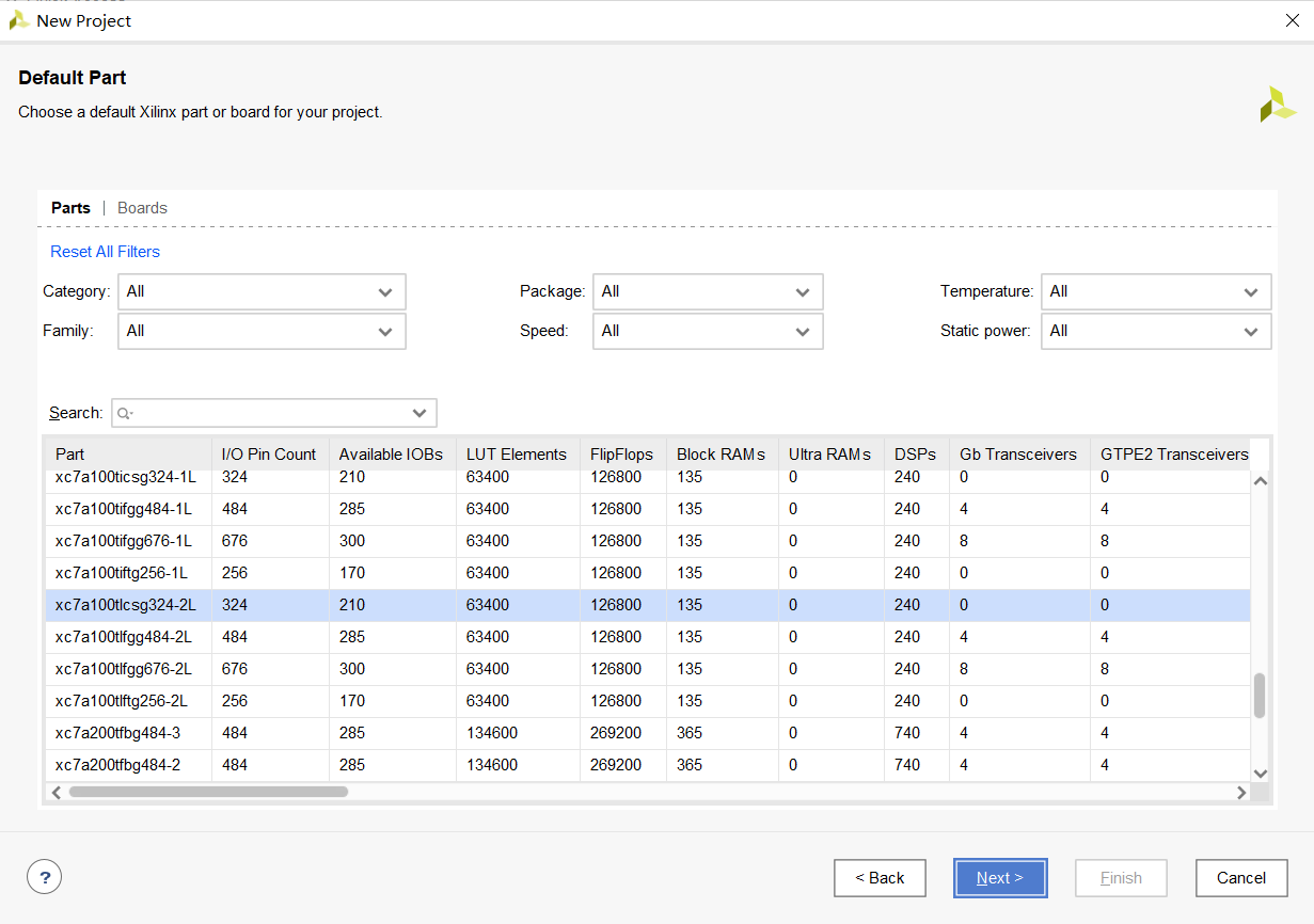
新建工程
选择xc7a100tlcsg324-2L板卡型号
1.结构描述建模全加器FA
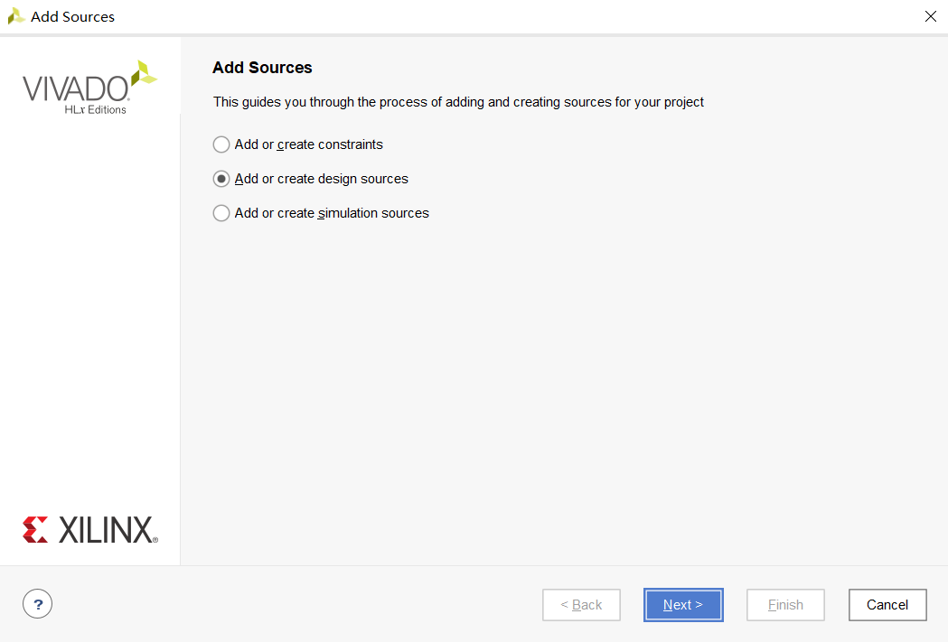
添加design sources
代码示例
1
2
3
4
5
6
7
8
9
10
11
12
13
|
`timescale 1ns / 1ps
module fa(A, B, CI, S, CO);
output S, CO;
input A, B, CI;
wire S1, T1, T2, T3;
xor XOR_1(S1, A, B),
XOR_2(S, S1, CI);
and AND_1(T1, A, B),
AND_2(T2, S1, CI);
or OR_1(CO, T1, T2);
endmodule
|
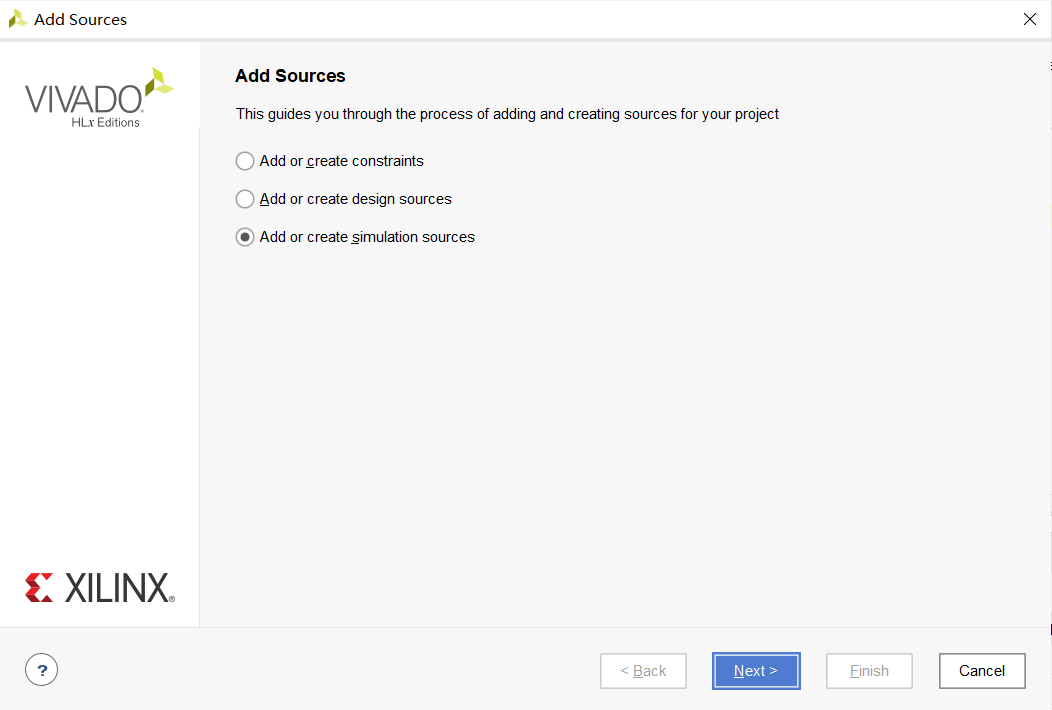
添加simulation sources
仿真代码示例
利用脚本自动输出
1
2
3
4
5
6
7
8
9
10
11
12
13
14
15
16
17
18
19
20
21
22
23
24
25
26
27
28
29
30
31
32
33
34
35
36
37
|
`timescale 1ns / 1ps
module tb_fa;
parameter PERIOD = 10;
reg A = 0 ;
reg B = 0 ;
reg CI = 0 ;
wire S ;
wire CO ;
fa u_fa (
.A ( A ),
.B ( B ),
.CI ( CI ),
.S ( S ),
.CO ( CO )
);
initial
{A,B,CI}=3'b0;
always
begin
#100;
{A,B,CI}={A,B,CI} + 1'b1;
end
endmodule
|
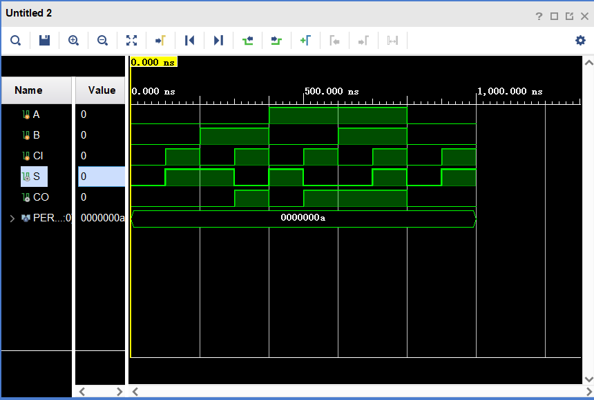
仿真结果
2.四位串行加法器
添加的design sources
PS:操作与前面相同
1
2
3
4
5
6
7
8
9
10
11
12
13
14
15
16
|
`timescale 1ns / 1ps
module FourBitFA(X, Y, Cin, Sum, Cout);
parameter size = 4;
input [size-1:0] X, Y;
output [size-1:0] Sum;
input Cin;
output Cout;
wire [size-1:1] C;
fa fa0(X[0], Y[0], Cin, Sum[0], C[1]),
fa1(X[1], Y[1], C[1], Sum[1], C[2]),
fa2(X[2], Y[2], C[2], Sum[2], C[3]),
fa3(X[3], Y[3], C[3], Sum[3], Cout);
endmodule
|
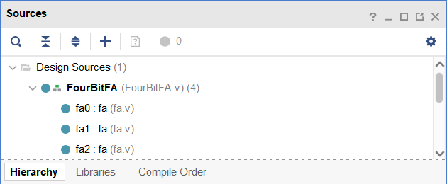
添加完之后,FourBitFA模块会自动置顶,并且包含fa模块
添加simulation sources
可由脚本自动生成(有删改)
1
2
3
4
5
6
7
8
9
10
11
12
13
14
15
16
17
18
19
20
21
22
23
24
25
26
27
28
29
30
31
32
33
34
35
36
37
|
`timescale 1ns / 1ps
module tb_FourBitFA;
parameter PERIOD = 10;
parameter size = 4;
reg [size-1:0] X = 0 ;
reg [size-1:0] Y = 0 ;
reg Cin = 0 ;
wire [size-1:0] Sum ;
wire Cout ;
FourBitFA #(
.size ( size ))
u_FourBitFA (
.X ( X [size-1:0] ),
.Y ( Y [size-1:0] ),
.Cin ( Cin ),
.Sum ( Sum [size-1:0] ),
.Cout ( Cout )
);
initial
{X, Y, Cin} = 9'b0;
always
begin
#100;
{X, Y, Cin} = {X, Y, Cin} + 1'b1;
end
endmodule
|
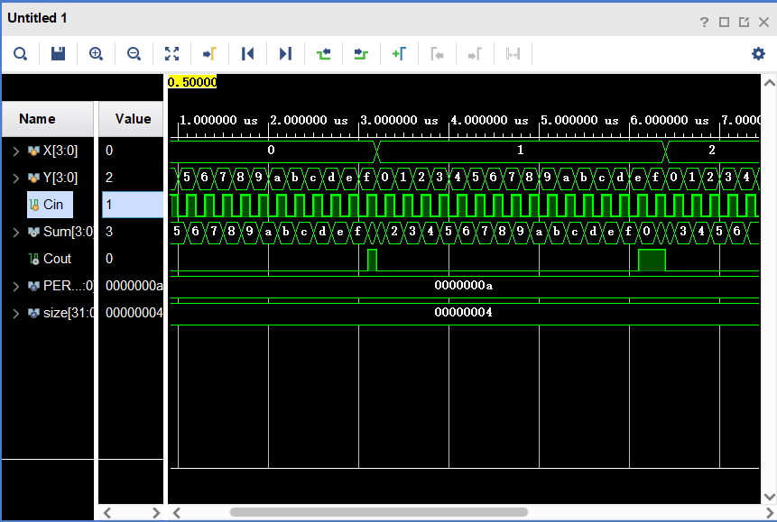
仿真结果
3.数据流法实现超前进位电路
添加design sources
1
2
3
4
5
6
7
8
9
10
11
12
13
14
15
16
17
18
19
20
21
22
|
`timescale 1ns / 1ps
module CarryAheadAdd(X, Y, Cin, Cout);
parameter size = 4;
input [size-1:0] X, Y;
input Cin;
output [size:0] Cout;
wire [size:0] C, G, P;
assign C[0] = Cin;
assign P = X ^ Y;
assign G = X & Y;
assign C[1] = G[0] | (P[0] & C[0]);
assign C[2] = G[1] | (P[1] & (G[0] | (P[0] & C[0])));
assign C[3] = G[2] | (P[2] & (G[1] | (P[1] & (G[0] | (P[0] & C[0])))));
assign C[4] = G[3] | (P[3] & (G[2] | (P[2] & (G[1] | (P[1] & (G[0] | (P[0] & C[0])))))));
assign Cout = C;
endmodule
|
4.四位超前进位加法器
添加design sources
1
2
3
4
5
6
7
8
9
10
11
12
13
14
15
16
17
18
19
20
21
22
23
|
`timescale 1ns / 1ps
module CarryAheadAdder(Sum, Cout, X, Y, Cin);
parameter size = 4;
input [size-1:0] X, Y;
input Cin;
output [size-1:0] Sum;
output Cout;
wire [size:0] C;
CarryAheadAdd CarryAheadAdd_0(X, Y, Cin, C);
fa fa0(X[0], Y[0], Cin, Sum[0]),
fa1(X[1], Y[1], C[1], Sum[1]),
fa2(X[2], Y[2], C[2], Sum[2]),
fa3(X[3], Y[3], C[3], Sum[3]);
assign Cout = C[4];
endmodule
|
添加simulation sources
1
2
3
4
5
6
7
8
9
10
11
12
13
14
15
16
17
18
19
20
21
22
23
24
25
26
27
28
29
30
31
32
33
34
35
36
37
38
|
`timescale 1ns / 1ps
module tb_CarryAheadAdder;
parameter PERIOD = 10;
parameter size = 4;
reg [size-1:0] X = 0 ;
reg [size-1:0] Y = 0 ;
reg Cin = 0 ;
wire [size-1:0] Sum ;
wire Cout ;
CarryAheadAdder #(
.size ( size ))
u_CarryAheadAdder (
.X ( X [size-1:0] ),
.Y ( Y [size-1:0] ),
.Cin ( Cin ),
.Sum ( Sum [size-1:0] ),
.Cout ( Cout )
);
initial
{X, Y, Cin} = 9'b0;
always
begin
#100;
{X, Y, Cin} = {X, Y, Cin} + 1'b1;
end
endmodule
|
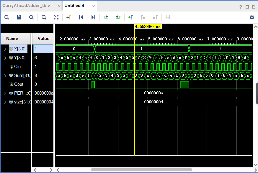
仿真结果
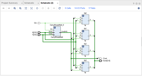
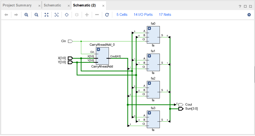
原理图(RTL分析)
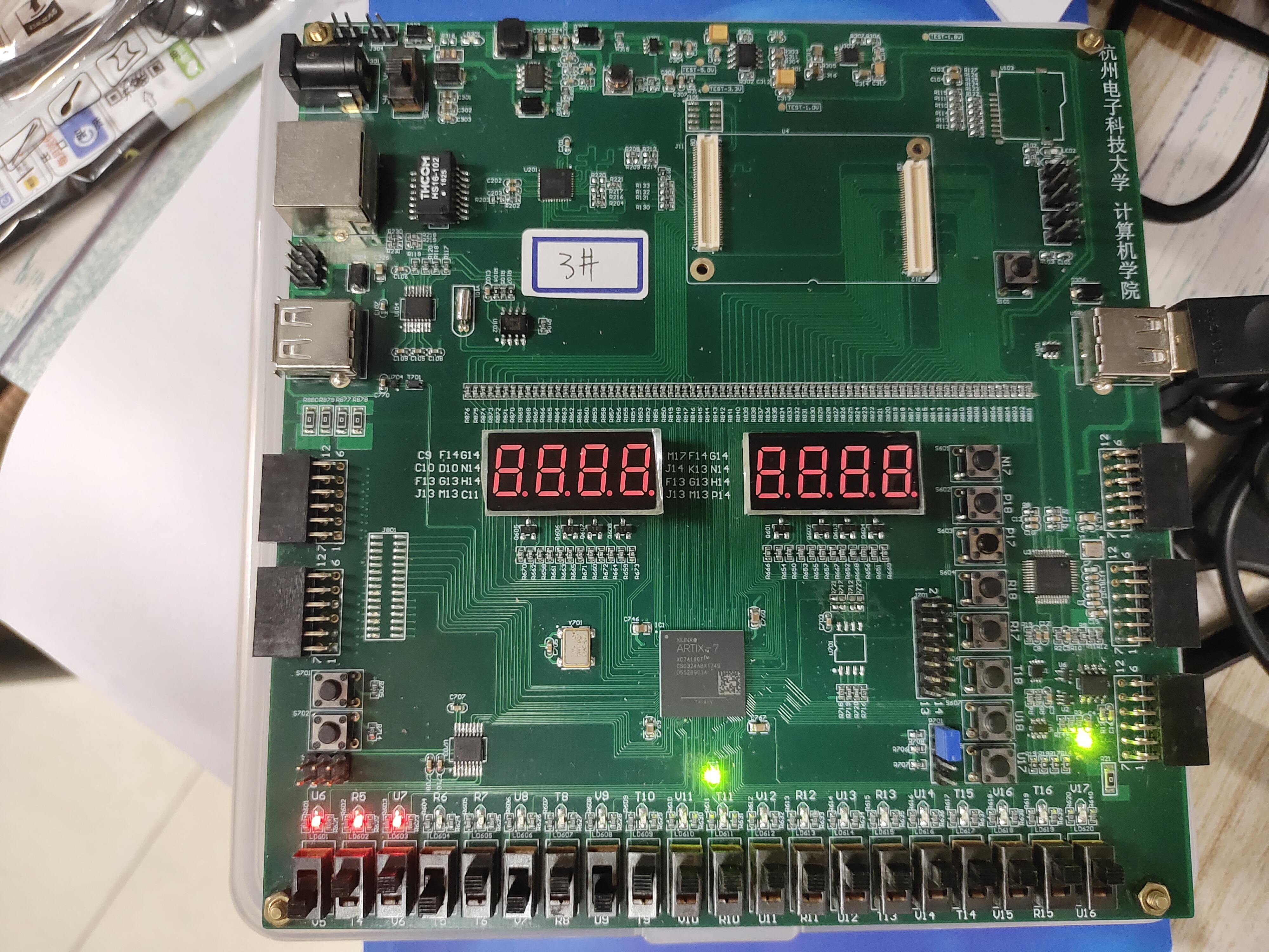
5.板级验证
经过综合、实现、比特流之后,编写管脚约束文件
1
2
3
4
5
6
7
8
9
10
11
12
13
14
15
| set_property IOSTANDARD LVCMOS18 [get_ports {X[3]}]
set_property PACKAGE_PIN V5 [get_ports {X[3]}]
set_property -dict {IOSTANDARD LVCMOS18 PACKAGE_PIN T4} [get_ports {X[2]}]
set_property -dict {IOSTANDARD LVCMOS18 PACKAGE_PIN V6} [get_ports {X[1]}]
set_property -dict {IOSTANDARD LVCMOS18 PACKAGE_PIN T5} [get_ports {X[0]}]
set_property -dict {IOSTANDARD LVCMOS18 PACKAGE_PIN T6} [get_ports {Y[3]}]
set_property -dict {IOSTANDARD LVCMOS18 PACKAGE_PIN V7} [get_ports {Y[2]}]
set_property -dict {IOSTANDARD LVCMOS18 PACKAGE_PIN R8} [get_ports {Y[1]}]
set_property -dict {IOSTANDARD LVCMOS18 PACKAGE_PIN U9} [get_ports {Y[0]}]
set_property -dict {IOSTANDARD LVCMOS18 PACKAGE_PIN T9} [get_ports Cin]
set_property -dict {IOSTANDARD LVCMOS18 PACKAGE_PIN U6} [get_ports {Sum[3]}]
set_property -dict {IOSTANDARD LVCMOS18 PACKAGE_PIN R5} [get_ports {Sum[2]}]
set_property -dict {IOSTANDARD LVCMOS18 PACKAGE_PIN U7} [get_ports {Sum[1]}]
set_property -dict {IOSTANDARD LVCMOS18 PACKAGE_PIN R6} [get_ports {Sum[0]}]
set_property -dict {IOSTANDARD LVCMOS18 PACKAGE_PIN R7} [get_ports Cout]
|
将程序下载到电路板
 wechat
 alipay